
![]()
Designed by: Vassilis Stergiopoulos
Published by: Vassilis Serasidis at 26.Jul.2010
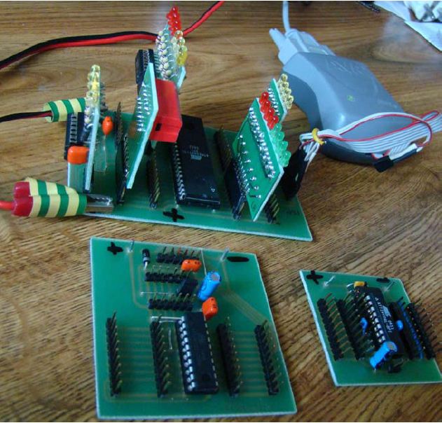
Picture 2: The experimental boards assembled.
General purpose experimental pcbs
Here are a few pcbs that provide simple experimental abilities for several AVR microcontrollers. Those shown can work with ATmega8515, ATtiny2313 and ATtiny26.
If we need other mpus we have to build the corresponding pcb. So for now, we have three pcbs, one for each of the above mpus. This way we don't need expensive development systems.
The name of the mpu is printed on the solder side, so now it reads opposite. When printed it should read normally.
We can divide those pcbs in two categories: (a) mpu pcbs, (b) peripheral pcbs. Cat-a pcbs are those that have a specific mpu, while cat-b pcbs are those that can be plugged to one of the cat-a pcbs. Cat-b pcbs contain LEDs (buffered or not) or switches. Of course we can construct more cat-b pcbs that will be more project oriented, like eeprom, other ICs, push buttons, etc.
Cat-a pcbs.
Mpus have ports, through which they communicate to the surrounding "world". We can see on cat-a pcbs, that each port has a separate connector / extension slot, where cat-b pcbs can be plugged. Each port has two paralleled extension slots, so that we can connect two cat-b pcbs at each port. Cat-a pcbs also have an ISP connection port. Normally it should be 2x3 pins arrangement, but I have modified it in 1x6 in order for the pcbs to be designed easily. You can modify the cable that comes with the AVRISP or other ISP programmer, so that it fits my arrangement. It is worth it. Or you can use a simple converter that you can easily build.
When we want to experiment, we choose the appropriate mpu and corresponding pcb, then we choose one or more extension pcbs, we connect the ISP, we apply 5volts stabilized power and we start experimenting.
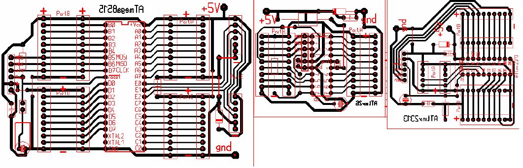
Picture 2: We see the three cat-a pcbs.
Cat-b pcbs:
As we said cat-pcbs can have LEDs, switches, push buttons, eeproms, or any other IC that is required for our project. So we need to construct additional pcbs, if we need more "peripherals".
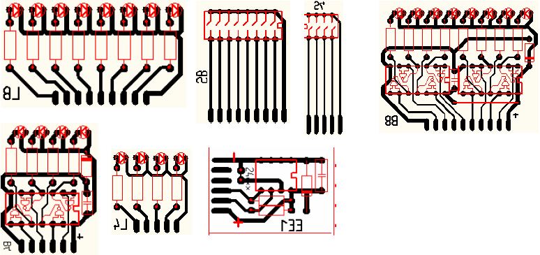
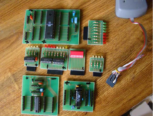
Picture 3: We can see several cat-b pcbs.
We also see that if a pcb needs power supply, it has a protection diode of the type 1N4001, against reverse power connection. This also protects the ISP programmer which is very sensitive to supply-voltage variations. Do not plug or unplug anything when the ISP programmer is connected and power is on. First switch the power source off.
As we can see each pcb has a name.
L4 pcb has four common-cathode LEDs with a series resistor each. We can plug this where no more than 4 LEDs are needed and no other component is to be connected to the same points in parallel. If this is not the case, we have to use a buffered pcb like B4, which provides 4 buffered LEDs. I have preferred to use the 4093 Schmidt-trigger NAND gates for buffering, that will work for sure, instead of a normal buffer, like 4001.
If we want to connect 5 to 8 LEDs then we must use the pcbs L8 or B8 depending if we want buffering or not.
The pcb named S4 it has just a 4-bank dip switch with common point.
The S8 has an 8-bank dip switch bank.
The pcb EE1 can accept a series EEPROM like 24CXX, where XX=01, 02, 04, 08. There is an optional jumper that you can insert, in case you want to try other programming modes of the chip. Then you must cut the shorting of the jumper.
Costruction
We notice that these cat-b pcbs, have edges without holes, since female pins are supposed to be soldered there.
See in the pictures. The female pins on cat-b pcbs have to be soldered vertically. These correspond to the male pins on the cat-a pcbs. The polarity of connection power is pointed on the pcbs.
Also a file with the above pcbs is included, in the sprint layout viewer software pcb-design format. It is called general.lay
Attention! Do not use direct switches to ports that have the ISP signals (MOSI, MISO and CLCK). If the switch is closed during ISP, the programmer may be damaged.
I have also included the file general.lay where the pcbs are drawn for the pcb sprint layout viewer software.
|
|
Download the source code in assembly, schematic and pictures of this project |
Created by Vassilis Stergiolpoulos and published by Vassilis Serasidis at 26.Jul.2010